


Our production capacity
| PCB Item | Manufacture Capacity |
| Layer Counts | 1--20L |
| Base Material | FR4,High-TG FR4,CEM3,aluminum,High Frequency(Rogers,Taconic,Aron,PTFE,F4B) |
| Material Thickness(mm) | 0.40, 0.60, 0.80, 1.00, 1.20, 1.50, 1.60, 2.0, 2.4, 3.2 |
| Max board size(mm) | 1200x400mm |
| Board Outline Tolerance | ±0.15mm |
| Board Thickness | 0.4mm--3.2mm |
| Thickness Tolerance | ±8% |
| Minimum line/space | 0.1mm |
| Min Annular Ring | 0.1mm |
| SMD Pitch | 0.3mm |
| Holes | |
| Min Hole Size(mechanical) | 0.2mm |
| Min Hole Size(laser hole) | 0.1mm |
| Hole Size Tol (+/-) | PTH:±0.075mm;NPTH: ±0.05mm |
| Hole Position Tol | ±0.075mm |
| Plating | |
| HASL/LF HAL | 2.5um |
| Immersion Gold | Nickel 3-7um Au:1-5u'' |
| Surface Finish | HAL,ENIG,Plated Gold,Immersion Gold,OSP |
| Copper | |
| Copper Weight | 0.5--6oz |
| Color | |
| Solder mask | Green, Blue, Black, White, Yellow, Red, Matt Green, Matt Black, Matt Blue |
| Silk screen | White, Black, Blue,Yellow |
| Acceptable File Format | Gerber file,Powerpcb,CAD,AUTOCAD,ORCAD,P-CAD,CAM-350,CAM2000 |
| Certificate | ROSH,ISO9001,UL |
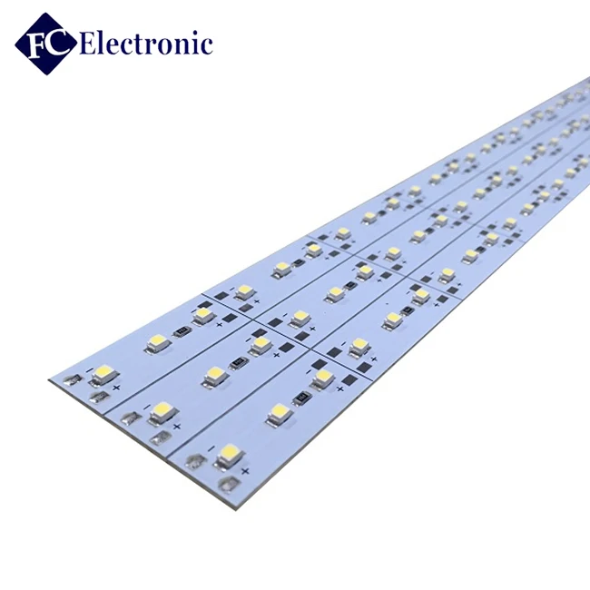
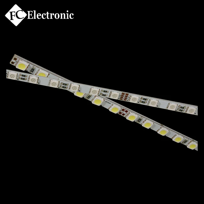
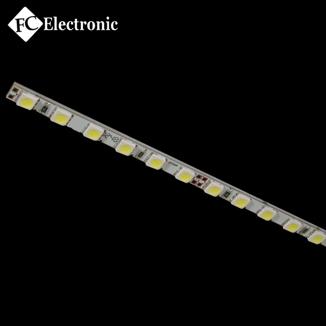
Pcb manufacture and assembly led tube light pcb , led strip pcb board

OEM/ODM/EMS Services for PCBA:
- PCBA, PCB Board assembly: SMT & PTH & BGA
- PCBA and enclosure design
- Components sourcing and purchasing
- Quick prototyping
- Plastic injection molding
- Metal sheet stamping
- Final assembly
- Test: AOI, In-Circuit Test (ICT), Functional Test (FCT)
- Custom clearance for material importing and product exporting
Capability - SMT
- Lines 9(5 Yamaha,4KME)
- Capacity 52 million placements per month
- Max Board Size 457*356mm.(18”X14”)
- Min Component size 0201-54 sq.mm.(0.084 sq.inch),long connector,CSP,BGA,QFP
- Speed 0.15 sec/chip,0.7 sec/QFP
Capability - PTH
- Lines 2
- Max board width 400 mm
- Type Dual wave
- Pbs status Lead-free line support
- Max temp 399 degree C
- Spray flux add-on
- Pre-heat 3
Android motherboard pcba according to BOM gerber files


To ensure an accurate quote, be sure to include the following information for your project:
•Complete GERBER files including the BOM list
•Other file types (Altium,Protel,OrCAD)
•"Read Me" notes for additional fabrication information
•Quantities
•Turn time
•Panelization Requirements
•Materials Requirements
•Finish requirements
Your custom quote will be delivered in just 2-24 hours, depending on the design complexity.
AOI Testing
Checks for solder paste
Checks for components down to 0201"
Checks for missing components, offset, incorrect parts, polarity
X-Ray Inspection
X-Ray provides high-resolution inspection of:
BGAs
Micro BGAs
Chip scale packages
Bare boards
In-Circuit Testing
In-Circuit Testing is commonly used in conjunction with AOI minimizing functional
defects caused by component problems.
Power-up Test
Advanced Function Test
Flash Device Programming
Functional testing
We purchase material from Original Company and distributers.
We make products by strict engineer processes.
We have strict inspection processes.
We send products by vaccum package,antistatic package and carton box.
1. Are my design files secure when I send them to you?
Your files are held in complete safety and security.Your files are never shared nor will any third parties have access to your design files.Fulltronics can sign an NDA(Non-disclosure agreement) before sending files.
2. For small quantity orders, can you produce prototype PCBs?
Yes. Fulltronics can produce prototypes. but the greater the quantity, the greater the cost savings.
3. What file formats do you accept for PCB and assembly?
Gerber ,CAM Auto CAD DXF, DWG formats.
4. Do you have after-sales product servicing available for your customers?
Yes, for any quality problems Fulltronics will take our responsibility to solve it for you any time.