


Welcome to HongTai!
PCB , PCBA , FPC , MCPCB
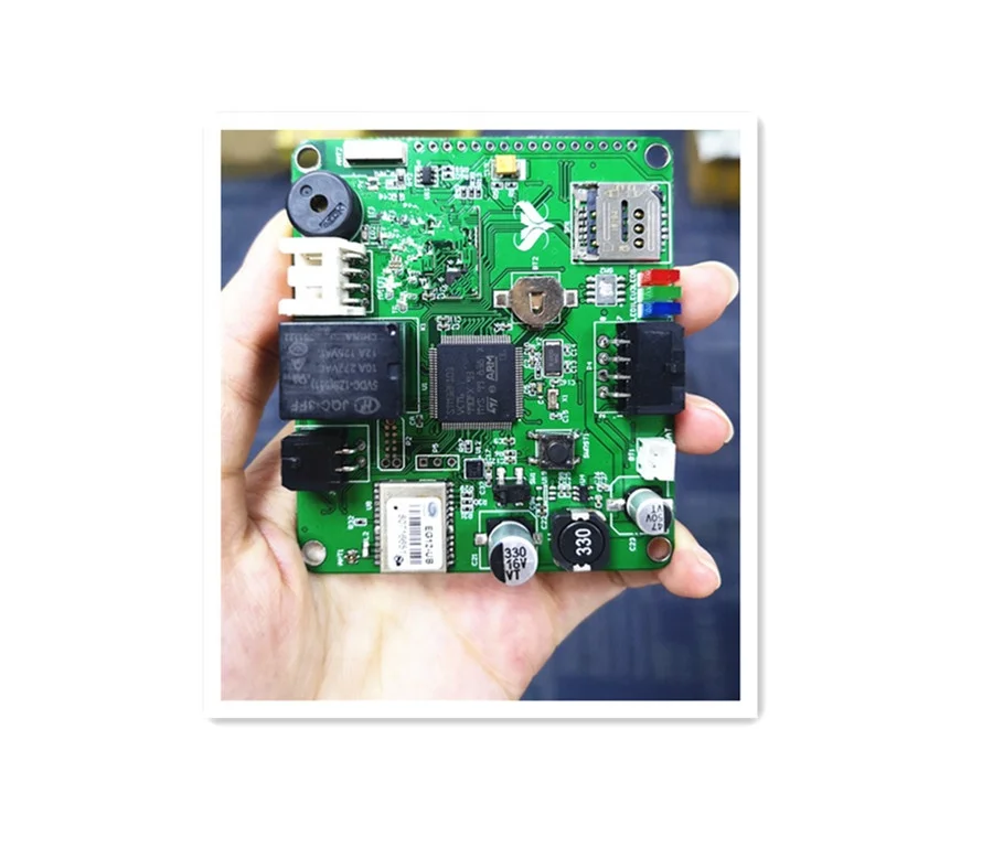
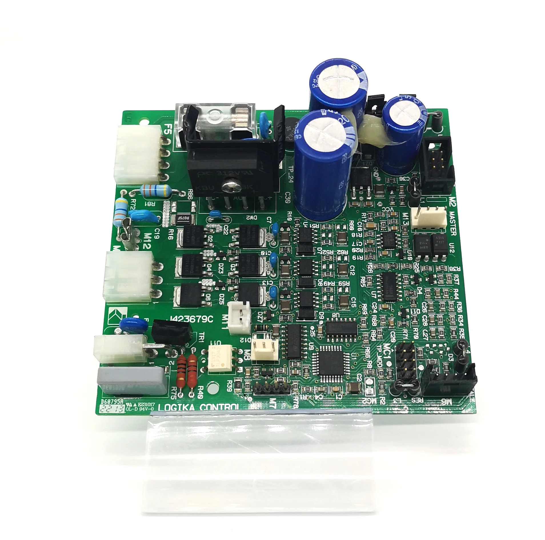
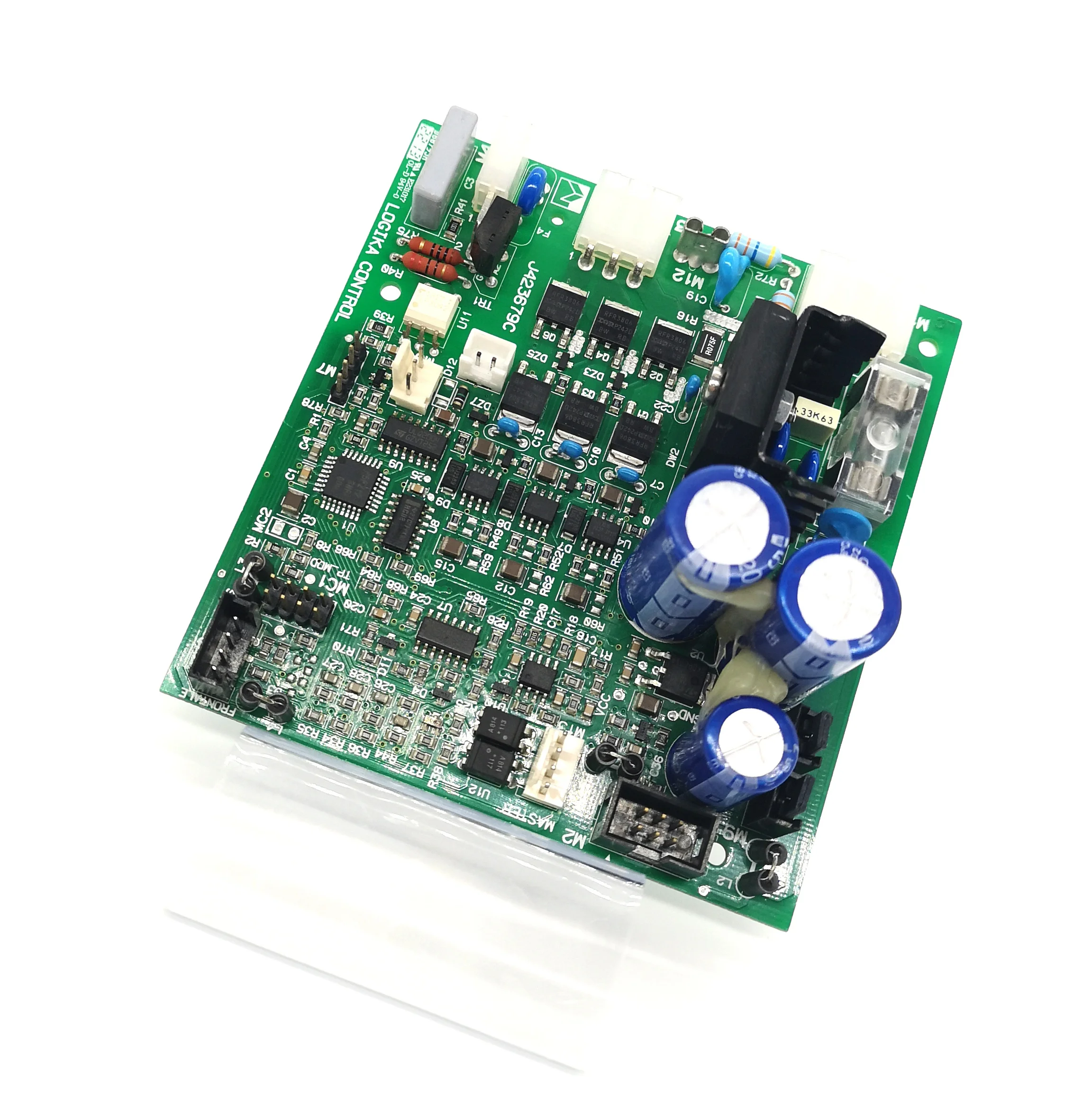
HongTai Technology Co.,Ltd is built up in 1997 to focus on the Electronic Manufacturing Services , which specializes in PCB fabrication and PCB Assembly , including FR4 PCB, Rogers PCB, Rigid-Flex PCB ,LED PCB , PCBA , MCPCB, FPC etc.
We offer one-stop service, consisting of reasonable quote, layout/design, copy (Gerber, BOM), fabrication, component sourcing, assembly (SMT, DIP, COB ), advanced testing, well packing, fast delivery and after-sales service.
Quality first, lead time second, NO MOQ , we shall start with prototype/sample
You are welcome to visit our website to know more:htpcba.com


We have professional PCB designer for your PCB layout requirement. We design single, double, and multi layers , Rigid, flexible, and Flex-Rigid printed circuit boards.
Our mature engineering methodology ensures efficient, cost effective designs, done right the first time.
We have extensive experience in creating RoHS compliant designs for new layouts and conversions of existing assemblies. Also, ask about our reverse engineering capabilities, as we can convert an existing board assembly without documentation into a complete and functional databas
Capabilities and Services offered:
1.Schematic capture
2. Assembly drawings, fabrication drawings
3. Board layout from a customer supplied schematic diagram
4. Reverse engineering
5. Controlled impedance (single and differential) designs
6. Layout for RF designs
7. High Speed Backplane and Mid-plane DesignsMicro BGA / Micro via/ Blind & Buried Vias
8. Multi-layer boards, split ground planes, differential pairs, high speed rules
9. Routing per trace/space, keep-out, and clearance rules specified by customer
10. Component resequencing based on physical layout, reverse annotation to schematic
11. DFT audit, test point placement, test probe clearance per customer rules, testability report
12. Surface mount or through hole designs
13.Unusual PCB shapes
We offer one stop EMS service, thus we can help you make the circuit layout and then make it produced.
FAQ.
Q1. If I want to get a PCB layout quote, what details should I provide?
A1. Please send us the schematics.
Q2. What is your layout service cost?
A2: Layout cost depends on the complexity of PCB. We can send you an exact quote when we receive your files and requirements.
| HongTai Technology Co.,LTD | ||
| Seq | Item | capability |
| 1 | Base Material | FR-4, High TG FR-4 , Halogen Free material ,CEM-3,CEM-1,PTFE,Rogers ,Arlon ,Taconic,Aluminum base,Teflon,PI ,etc |
| 2 | Layers | 1-40 ( ≥30 layers needs review ) |
| 3 | Finished inner/outer copper thickness | 0.5-6OZ |
| 4 | Finished board thickness | 0.2-7.0mm(≤0.2mm needs review),≤0.4mm for HASL |
| Board thickness≤1.0mm: +/-0.1mm 1<Board thickness≤2.0mm: +/-10% Board thickness>2.0mm: +/-8% |
||
| 5 | Max panel size | ≤2sidesPCB: 600*1500mm Multilayer PCB: 500*1200mm |
| 6 | Min conductor line width/spacing | Inner layers: ≥3/3mil Outer layers: ≥3.5/3.5mil |
| 7 | Min hole size | Mechanical hole: 0.15mm Laser hole: 0.1mm |
| Drilling precision: first drilling First drilling: 1mil Second drilling: 4mil |
||
| 8 | Warpage | Board thickness≤0.79mm: β≤1.0% 0.80≤Board thickness≤2.4mm: β≤0.7% Board thickness≥2.5mm: β≤0.5% |
| 9 | Controlled Impedance | +/- 5 % Ω(<50Ω),+/-10%(≥50Ω),≥50Ω+/-5% (needs review) |
| 10 | Aspect Ratio | 15:01 |
| 11 | Min welding ring | 4mil |
| 12 | Min solder mask bridge | ≥0.08mm |
| 13 | Plugging vias capability | 0.2-0.8mm |
| 14 | Hole tolerance | PTH: +/-3mil NPTH: +/-2mil |
| 15 | Outline profile | Rout/ V-cut/ Bridge/ Stamp hole |
| 16 | Solder mask color | Green,yellow,black,blue,red,white,matte green |
| 17 | Component mark color | white,yellow,black |
| 18 | Surface treatment | OSP: 0.2-0.5um HASL: 2-40um Lead free HASL: 2-40um ENIG: Au 1-10U’’ ENEPIG: PB 2-5U’’/ Au 1-8U’’ Immersion Tin:0.8-1.5um Immersion silver: 0.1-1.2um Peelable blue mask Carbon ink Gold plating: Au 1-150U’’ |
| 19 | E-Test | Flying probe tester : 0.4-6.0mm,max 19.6*23.5inch |
| Min spacing from test pad to board edge : 0.5 mm | ||
| Min conductive resistance : 5 Ω | ||
| Max insulation resistance : 250 MΩ | ||
| Max test voltage : 500 V | ||
| Min test pad diameter : 6 mil | ||
| Min test pad to pad spacing : 10 mil | ||
| Max test current : 200 MA | ||
| 20 | AOI | Orbotech SK-75 AOI : 0.05-6.0mm,max 23.5*23.5inch |
| Orbotech Ves machine : 0.05-6.0mm,max 23.5*23.5inch | ||
To give you an exact quote, we hope you could offer us listed infomation.
1. PCB : Gerber file and other PCB files.
We would appreciate if you can confirm listed PCB specification also.
1). material 2). board thickness 3). copper thickness 4). surface finishing 5). soldermask color 6). silkscreen color
2. PCBA : PCB files and BOM list
3. If you don't have ready design files, you can send us a sample, then we will clone for you.
4. We also offer custom PCB design and modify service.

