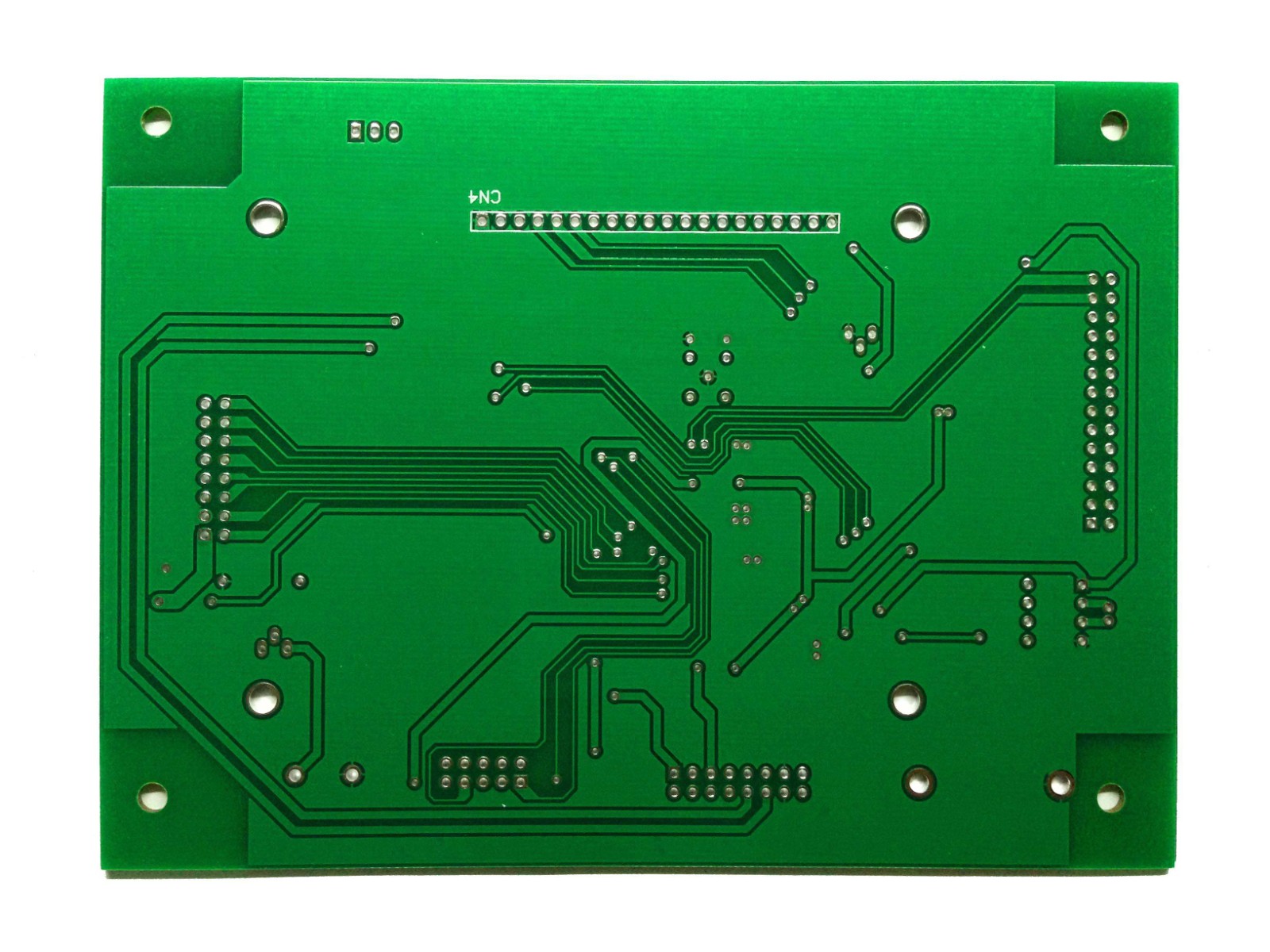
Warpage in the manufacture of printed circuit boards can cause inaccurate positioning of components; when the board is bent in SMT and THT, the components are not properly inserted, which will bring difficulties to PCB assembly and installation work.
IPC-6012, SMB--SMT printed circuit board maximum warp or distortion of 0.75%, other board warp generally does not exceed 1.5%; electronic assembly plant allowed warp (double / multi-layer) is usually 0.70 ---0.75%, (1.6mm plate thickness) In fact, many boards such as SMB, BGA board requires warp less than 0.5%; some PCB manufacturers even less than 0.3%;

Warpage calculation method = warpage height / curved length
Prevention of PCB board warpage:
1、Engineering design: the inter-layer prepreg arrangement should correspond; the multi-layer core board and prepreg should use the same supplier product; the outer C/S surface area should be as close as possible, and a separate grid can be used;
2、Drying before baking: generally 150 degrees 6-10 hours, remove the water vapor inside the plate, further cure the resin completely, eliminate the stress inside the plate; bake the plate before opening, whether it is inside or both sides!
3、Warp and weft shrinkage ratio is different,pay attention to the warp and weft direction before laminating the sheet;when the core board is blanked, attention should also be paid to the warp and weft direction; the direction of the solidified sheet coil is the warp direction; the long direction of the copper clad plate is the warp direction.
4、Laminating thick to relieve stress, cold pressing after pressing plate, trimming raw edges.
5、Boiler before drilling: 150 degrees 4 hours.
6、The thin plate is preferably not mechanically brushed, it is recommended to use chemical cleaning; special fixture is used for plating to prevent the board from bending and folding.
7、After the tin is sprayed, it is naturally cooled to room temperature on a flat marble or steel plate or the air floating bed is cooled and cleaned;
Warping plate treatment: 150 degrees or hot pressing for 3-6 hours, using a smooth and smooth steel plate, 2-3 times baking.

