

 Share
Share


Brand: |
none |
Address: |
China |
Min.Order: |
none |
Supply: |
none |
Valid until: |
Long Term |
Product Details


General Descriptions
1 Introduction
The M104GNX1 R1 is a color active matrix thin film transistor (TFT) liquid crystal display (LCD) that uses amorphous silicon TFT as a switching device. This model is composed of aTFT LCD panel, a driver circuit and a backlight system. This TFT LCD has a 10.4 inch diagonally measured active display area with XGA resolution (1,024 horizontal by 768 vertical pixels array).
2 Features
- Supported XGA Resolution
- LVDS Interface
- Compatible with RoHS Standard
3 Product Summary
Product Name | IVO M104GNX1 R1 Industrial 10.4" Lcd Module |
Model | M104GNX1 R1 |
Size | 10.4inch |
Resolution | 1024*768 |
Pixel Pitch (H x V) | 0.2063 x 0.2063 mm |
Brightness(nits) | 350 |
Pixel Arrangement | R.G.B. Vertical Stripe |
Display Mode | Normally White |
Contrast Ratio | 900:1 |
| Response Time | 16 ms |
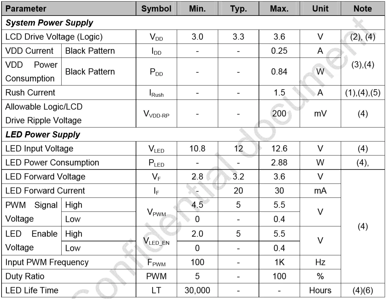
| Input Voltage | 3.3 v |
| Power Consumption | 3.72W |
| View Angle(L/R/U/D) | 75/75/75/75 |
| Response Time(ms) | 16ms |
| Optical mode | TN |
| Operating Temperature | -20°-70° |
| Storage Temperature | -30°-80° |
| Interface | LVDS/6/8-bit |
| Lamp type | LED |
| LED Life Time(Hrs) | 15,000Hours |
| Active Area(mm,H*V) | 211.20*158.40 |
| Outline Dimension | 236.00*176.90*5.70 |
Weight | 300g |
Support Color | 262 K/16.7 M |
NTSC | 50 (Typ.) |
Viewing Direction | 6 O’clock |
Surface Treatment | Anti-Glare |
Authentication | ROSH/UL |
The following parts are optional. If you need them, welcome to make an inquiry,I will give you best price.
4 Definition of Viewing Angle
5 Signal Connector Pin Assignment
| Pin No. | Symbol | Description |
| 1 | VDD | Power Supply, 3.3V (typical) |
| 2 | ||
| 3 | VSS | Ground |
| 4 | REV | Reverse Scan selection {High:2.5(min), 3.3(typ),3.6(max); Low: 0.5(max)} |
| 5 | Rin1- | -LVDS differential data input (R0-R5,G0) |
| 6 | Rin1+ | +LVDS differential data input (R0-R5,G0) |
| 7 | VSS | Ground |
| 8 | Rin2- | -LVDS differential data input (G1-G5,B0-B1) |
| 9 | Rin2+ | +LVDS differential data input (G1-G5,B0-B1) |
| 10 | VSS | Ground |
| 11 | Rin3- | -LVDS differential data input (B2-B5,HS,VS,DE) |
| 12 | Rin3+ | +LVDS differential data input (B2-B5,HS,VS,DE) |
| 13 | VSS | Ground |
| 14 | CIkIN- | -LVDS differential clock input |
| 15 | CIkIN+ | +LVDS differential clock input |
| 16 | GND | Ground |
| 17 | Rin4- | -LVDS differential data input (R6-R7,G6-G7,B6-B7) |
| 18 | Rin4+ | +VDS differential data input (R6-R7,G6-G7,B6-B7) |
| 18 | SEL68 | 6/8 bits LVDS data input selection(H:8bits L/NC:6bits) |
| 20 | Bist | Internal use |
Note(1) REV=LOW/NC
6 LED Connector Name / Designation
| Item | Description |
| Manufacturer/Type | STM/MSB24038P5A |
| Mating Receptacle/Type (Reference) | P24038P5 |
7 LED Connector Pin Assignment
| Pin No. | Symbol | Signal name |
| 1 | VCC | 12V |
| 2 | GND | GND |
| 3 | ON/OFF | 5V-ON,0V-OFF |
| 4 | Dimming | PWM Dimming or Analog Dimming |
| 5 | NC | NC |
8 Input Power Specifications
9 Reference Outline Drawing (Front Side)
10 Reference Outline Drawing (Back Side)
Customer Reviews total 0 items